
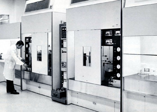
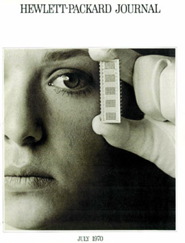
Remembering Early Times at HP

HP Memories
How LEDs Evolved from Geek Playthings to
the Global Lighting Solution in Six Decades
by Bob Steward
Foreword
Mr. LED Solutions - Bob StewardThis HPMemory.org archive now features two memoirs by engineers who worked in the HPA components division at HP. John Uebbing was first to publish, in May, 2014 to record his life story in exploiting the semiconductor and optoelectronic technologies, like light-emitting-diodes and fiber optics. This second fascinating story by Bob Steward is very personal to me. I hired Bob from Stanford, back in 1969. We were struggling to prove that we could build a profitable business out of light-emitting diodes, made into numeric and alphanumeric displays. There were two tiny groups--as projects go at HP--one was led by George Kaposhilin, who was building little red lamps, previously called pilot lights. I led a separate group called the LED Display Department. I think Displays had a total of 10 people, including the materials production and assembly folks. One of my engineers was a clever and innovative whiz named Joe Diesel. Joe worked primarily on production fixtures and test equipment that streamlined the physical processes that our assembly people used to fabricate these tiny magical wonders. But we needed a circuit designer, for the product applications, for the expertise to create the decoder IC chips, as well as to work with customers who needed to build external strobing driver circuits into their own uses of LED digits. That is where Bob Steward came in, a brand newly minted MSEE from Stanford. And very typical of the talent and skills that were coming into the exciting semiconductor technologies of those years. Our first HP 7000 display product was a 1/4th inch numeric digit, packaged behind a "hermetic" glass window, about an inch high. The digit was formed with 28 miniscule chips (we called them die) in a 5 x 7 pattern, driven by an onboard decoding integrated circuit. Each of those tiny light emitting die was 21 thousands of an inch square, about the size of a grain of table salt. So our assemblers attached them to the ceramic base, under a microscope with hand-held tweezers. That ceramic was a tiny printed circuit board, wired to the IC and power and data. Frustrations with the Gallium-Arsenide-Phosphide materials were the order of the day. The 7000 price was listed at $75 EACH digit. Our first big order came from Longines, the Swiss watch maker which had designed a handheld race timer, each with 4 digits. I think we gave them a quantity price of $25 each for maybe 1000 units. That got us some revenue, and the confidence to get production going. But obviously we needed a cheaper model. This required new design talent, in particular to design the decoder IC for a new model, the 7300. That model used fewer die, in a 4 x 7 matrix. As you will see from Bob's memoir, the production processes of that period were maddening. The companies like Fairchild and Advanced Microsystems, which processed silicon, were getting their processes under control technically. But our work with gallium metal and two poison nerve gases, arsine and phosphine, was anything but ordinary. By the time the magical combination of those three elements became a solid crystal, and got converted into a diode, which would generate red light, we had gone through maybe 32 individual process steps. Any one of which, done wrong, could yield a lot of expensive little chips with zero light. And there were a lot of chips with no light. That small team of people really did have a vision of the future. As the HP-35 scientific calculator rolled out in 1972 to worldwide acclaim, we knew that there were many applications like that, which could ONLY be solved with tiny lighted semiconductors. We were already designing other numeric and alphanumeric configurations to meet other user requirements. Bob's narrative walk through all those various product formats shows just how inventive were the engineers in that team. Being a part of the large Hewlett Packard instrument and computer company also offered so many new product opportunities. So many measurement and generator instruments needed some sort of display, either of the measurement or of some parameter in the instrument, such as the frequency of a signal source. This was not to say those sales were automatic - engineers like Bob needed to consult with the instrument engineers, to design LED driver circuits which could power up the red numbers, with the right data inputs and proper electric driver sources. The final products needed not just a technical number display, but they had to look good aesthetically. So there was a style aspect to a numbered digit, maybe the numbers like 0 needed a very slight "barreling" to the appearance, to soften the hard edges that happened with straight lines. While we weren't flying blind, we did recognize that these products had an industrial design factor that was important. Engineers had to pay attention. Bob's LED career at HP, Agilent, and Lumileds spanned so many decades that he worked on a range of technologies. As HP corporate moved into inkjet printers, the demand for a highly-precise paper drive motor emerged. Consider that the inkjet technique consists of a printer head that blasts out minuscule droplets of ink, maybe 1000+ per inch. So, when doing graphics, the printer head passes back and forth, so the dots have to line up both horizontally and vertically precisely to avoid discontinuity lines. Bob was involved in those innovative applications of LED emitter/detectors, which enabled the HP dominance of global printer business for decades. Later, in his years with the HP-Philips partnership, Lumileds, he participated in some of the most audacious visions for energy-saving light "bulbs”. Philips is a giant company, of General Electric stature, and serves the illumination business, probably since the creation of the filament light bulb. Their vision of "power illumination" using the LED, and blue LED-pumped phosphors has enabled a revolution in modern lighting. From the lighting for homes to commercial to industrial to automotive to city streets, these energy-efficient semiconductors are paving the way to the future, reducing the global need for power generation and the attendant impact on global warming. Bob was instrumental in those technology moves. It is fascinating to read of these years of technology ferment. Young brains, turned loose on some vexing problems, both technical and production oriented. Think of it this way. If these teams of creative people had not dedicated their lives to LEDs, fiber optics, laser diodes and detectors, there would be no cell phone displays, flat screen televisions, Internet communications, smartPads, or any of the dozens of modern necessities that we all take for granted. I, for one, say thank you Bob, and our other Memoir author John Uebbing.
John Minck
|
![]() Click here to download Bob's memories in PDF format - The 32 pages document is a 900 kb PDF file.
Click here to download Bob's memories in PDF format - The 32 pages document is a 900 kb PDF file.
How LEDs Evolved from Geek Playthings to
the Global Lighting Solution in Six Decades
by Bob Steward
My Early Years
I was around 6 when my appetite for electronics was literally sparked by watching a 3 story high, very high voltage electric arcing Jacob’s Ladder - that would put it in 1952. Who knew it would lead to a six decade career with LEDs, or that that initial LED geek plaything in 1969 would become a mainstream global lighting technology, enabling never before possible applications and a reduction in the need for power plants and their impact on global warming.
My dad worked at Jennings Electronics, a company that designed and manufactured very high voltage switches and capacitors for utility companies for their 100,000 Volt power lines. During family day, they would set up high voltage nut crackers and a crackling 3 story tall Jacob Ladders with rising electric arcs spanning across 10 feet.
My dad was an electronics engineer, although he never finished college due to the Great Depression. He started at the University of Santa Clara, and then went to San Jose State because it was cheaper. Finally, he had to leave college to work to help support his parents. My father-in-law, who went to Cal, was not able to finish college either, for the same reason. My dad studied architecture in college, which was useful later when he designed and built his own mid-century modern house. As a teenager, dad had become a licensed Amateur Radio Operator so it was natural for him to become an electronics technician when he had to leave school. He just learned electronics design by experience. He ended up retiring as Vice President and Director of Engineering of Jennings Electronics (later ITT-Jennings) and held over 50 patents as the primary or sole inventor. Dad was in the power side of electricity, which was an interesting contrast to my field of microelectronics.
My mom graduated from Healds Business School and was the executive secretary at the San Jose Chamber of Commerce for many years. She switched to full time mom once they started a family. School and academics were important as she saw the barriers my dad had faced from not having a college degree.
There is a lot of local history in our family as I am a third-generation Californian, born in San Jose. My grandmother was about 18, living in San Francisco with her parents, during the great 1906 earthquake. Through her and my parents, who were both born in the South Bay Area, I’ve had a great oral history of the Bay, and what life was like here for all those decades. As well as living here all my life.
Home life for me was busy with a lot of family time and playing with the neighbors’ kids on our street that ended in an orchard near downtown San Jose. Besides school, I was active in music (trombone) and competitive swimming. I picked up the trombone again later around 1980 to play in the Monotones, a small band that played at HP OED for several years for birthdays and other events. I dusted off the trombone starting in 2013 to play in the San Jose High Alumni band as part of the high school’s 150th anniversary parade and on-going school events. Frequent Boy Scout activities provided invaluable leadership training and life skills as I earned my Eagle Scout Award. Later I would give back as a Scoutmaster who had a hand in over a dozen boys earning their Eagle Scout rank, including my son.
My parents’ family was small with all my relatives fitting around a dining room table. This was a marked contrast to my future wife’s family where the local annual family reunion drew more than a hundred. Judy’s extended family was so warm and welcoming – they quickly became my family too.
Judy Gomes and I were high school sweethearts. We were married in the Stanford Memorial Church and will celebrate 45 wonderful years of marriage this August. Judy earned her Bachelor’s Degree and teaching credential at San Jose State, and was a full time mom once we started our family.
San Jose State and Stanford
I would become the first person in my extended family to graduate from college. After graduating from San Jose High, I went to San Jose State for my BSEE. Balancing the academics at SJS was my active membership in Alpha Phi Omega, a national service fraternity based on the values of Scouting. We were the key service organization at San Jose State and responsible for the Homecoming Bonfire, Turkey Trot race, managing the registration lines (in the days before on-line registration), Used Book Stand, etc. And, of course, lots of parties and daily lunch-time bridge games in the Cafeteria. I was fortunate to earn a full-ride fellowship to Stanford as a National Science Foundation Fellow where I earned my MSEE. Stanford was a new experience. I went from #1 in my EE graduating class to being challenged to keep up with the best of the best.
Stanford was at the forefront of transistor, digital logic, and IC design, so I took a heavy load. Only later did I find out that some students would audit the toughest classes before taking them later for credit. But a great all around experience and I formed close ties to the school that continue today. This was reinforced when our son attended Stanford, earning his BSEE and MSEE in high speed analog circuit design. He is currently a Director of Analog Design at Linear Technology. Our daughter, Erin, earned her BS in Industrial Engineering from Arizona State and worked in production control and optimization at Maxim Integrated Products, leaving Maxim to become a full time mom when she and her husband started their family.
Joining HP
While at Stanford, I took a class on digital logic from a professor who was part of HP Labs. He became a key contact when I had to leave school to find a job, and join the National Guard to avoid being drafted for service in Vietnam (in 1969 the draft boards were actively going after grad students - the draft order was based on the month and day of your birth, and I had a low number). My professor connected me with HP Recruiting who set up the interviews. I was scheduled at both the IC Design area of Santa Clara Division and the new optoelectronics area that was part of HP Associates Division. The interviews at HP Associates were in the morning, sponsored by John Minck. That afternoon, I was in my first interview at Santa Clara Division with Max Schuller when John called Max to say he was going to offer me a job. So Max stopped his interview and told me to expect an offer. Howard Borden, who reported to John, was my first manager at HP; and I started in September of 1969. John ran that small department for about 3 years, and then moved to another division, and later ended back in the Microwave Division marketing communications. He subsequently penned a great story of his HP career work experiences, A Narrative History of Hewlett Packard, which is archived on this HPMemory.org website.
The Birth of HP Associates
The background behind LEDs at HP is an interesting one. The way HP Associates started is that Bill, Dave, Jack Melchor and a few other customers needed a high frequency diode, a high frequency component for our counters. Melchor had previously founded a system product company called Melabs. They did quite a lot of military contracting. He was at the time one of the early venture capital investors in Silicon Valley, and also instrumental in founding El Camino Hospital.
They couldn't find high performance microwave components that they needed, so they funded a start-up partnership that would provide these parts for HP and for outside sale. That happened in the early '60s. Soon, as HP stock went public on the NYSE, HP decided to merge those business interests into HP by buying out several similar partnerships with HP stock. That was how HP Associates became HP Associates Division, shortly before I joined them. It was, therefore, the natural site for LED work since they were already active in semiconductor type components. HPA had also produced photo-conductor components with one important application at HP Santa Clara as part of a data-converter/driver which took the BCD information from a decade counter module and drove the 10-line NIXIE digital display tubes.
 |
A disassembled NIXIE Tube, showing the 10 individual wire electrodes |
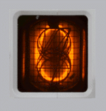 |
Same as above . . . . . . Still working |
There were two optoelectronics groups at HPA in 1969, both quite small operations. One was primarily making LED lamps, one chip per lamp - in reality, high reliability red pilot lights. They were red Gallium Arsenide Phosphide (GaAsP) chips. There must have been four or five engineers outside of the wafer fab (fabrication) area, and probably four or five engineers inside making the LEDs themselves. This was the original LED material - dim, deep-red chips. When I arrived, they had just transferred from HP Labs the first solid-state numeric display, the HP 7000 display. Along with the prototype product, came Howard Borden, who was the research scientist, and Gerry Pighini, the manufacturing manager.
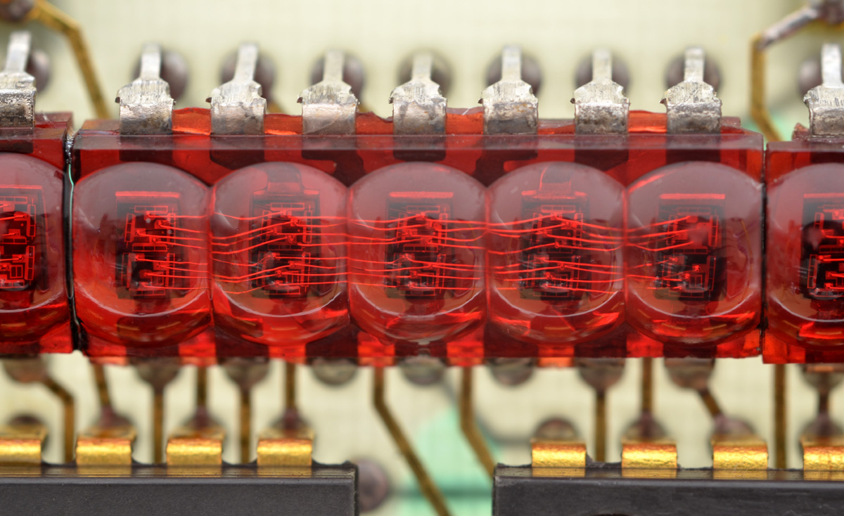
Why was HP interested in numeric and alphanumeric displays to begin with? At that time, HP was the biggest consumer of NIXIE® tubes. At least half of the HP product line was devoted to measurement instruments, and almost all of them required a readout - a meter, in some cases CRT tubes, and often a digital display. NIXIEs were well documented to be fragile. They were gas filled vacuum tubes consisting of 10 individual wire electrodes, each shaped to form a numeric character that lit up as a gas-glow numeral. The wires were stacked, one behind the other, zero through nine. This stacking produced a poor appearance because if you read them from the side you saw the parallax between adjacent digits, as well as creating a bulky display.
So, NIXIE tubes were expensive, fragile, bulky, and they had this parallax issue affecting appearance. Plus, they required a higher voltage to operate than the new evolving transistor technology which ran on 12-20 volts. In addition to the extra power and cost, switching of these special higher voltage power supplies introduced electrical noise inside an instrument which often was trying to make high precision, sensitive measurements. As a result, NIXIE tubes were not conducive to display data in any kind of modern instrument. So, the idea of LEDs and solid-state light sources really aligned with HP's corporate strategy -- not so much for lamps, which was the entry point to make something simple -- but really to create solid-state displays for a broad array of measurement instruments, for example, the frequency setting of an RF signal generator.
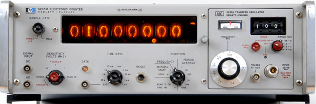 |
| Typical 8-digit NIXIEs Display of a HP 5245M Electronic Counter |
The Birth of the First LED Digit
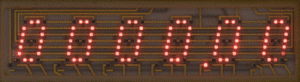
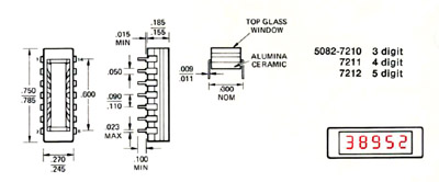
The 5082-7000 was HP’s first LED display (The XXXX-XXXX number format was HP's definition of purchased parts). The 5082 series was assigned for LED displays even though we were selling both internally to HP and externally to regular customers. We always talked in shorthand as just the 7000. The product was designed in HP's central research labs and was not simple to manufacture. HP Labs probably had not been too aligned with what was going on in semiconductor manufacturing. It had very thin, five mil (.005 inch) wispy, flat leads, which were easily broken, coming out of a ceramic package with a glass lid. Worse yet, the decoder IC inside used negative logic (a "1" is a low voltage, opposite to the emerging TTL IC logic) and non-standard voltage levels. This was all at a time before the industry had really shaken out to what was to become standard TTL logic.
The HP 7000 numeric display used a 5 x 7 array |
The 7000 used 28 small individual dots of LEDs. The numeric display had some shape to it, and was quite pleasing to read, although stacking more than one digit sideways showed numbers that were quite separated. It was much better looking than the later seven segment displays, which gave a brusque--albeit cheap--digit product. More on that later. By mounting red LEDs behind a red plastic filter, only the number appeared to the reader.
The easiest hybrid package to design and prototype at that time was just a ceramic substrate with a glass window. That configuration protected everything, and you didn't put any stresses around the wires, as occurred in the lower cost lamps with their encapsulated epoxy packages. If you have a single chip lamp with a single wire bond and when one breaks, you throw it away. It's okay. Not so, when you've got 28 chips per digit or a multi-monolithic chip display.
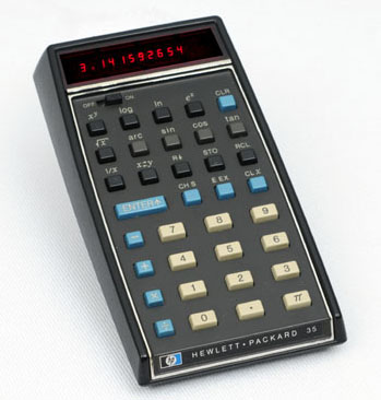
We found quickly that work was needed to come up with a more useable version of it. I was brought in to design the IC because that had been the specialty that I had taken at Stanford. I worked on the next generation of solid-state displays, as well as quickly got into the monolithic displays. The monolithics became part of the world renowned HP-35 scientific calculator. And John Minck's memoir does a good job of describing some of that activity. I won't duplicate what John described in his notes, but will add later some observations on the project, people and products that emerged.
Semiconductors were already in common use in other optoelectronic applications like emitters of infrared light. Or for use as photo-detectors which were sensitive to various wavelengths. Basic research into finding and optimizing materials which emitted visible light had been done at companies like GE, RCA, Bell Labs, and IBM.
The terminology III-V (verbally 3-5) comes from the periodic table of elements. Silicon and germanium are in the column IV group of materials. By combining elements from the third and the fifth columns, you get a combination crystal which can be processed into a light emitting semiconductor called Gallium Arsenide. These material combinations are also called Compound Semiconductors, to differentiate from the more common Silicon and Germanium materials.
Nick Holonyak Jr., while working at General Electric Company, first reported his visible-spectrum (red) LED, in the journal, Applied Physics Letters, on the December 1, 1962. He probably gets the title, "father of the light-emitting diode." Monsanto had been doing some very excellent work, primarily in the Midwest on the GaAs material side, and HP saw a strong need for that product. Both companies believed that they needed more critical mass to get the LED materials technology to the point where it could be commercialized. They agreed to jointly develop the material technology to the point where it had critical mass. After that, they would split and avoid any antitrust, anti-competition issues.
Following the fundamental work, both Monsanto and HP proceeded with the commercial material development on their own. Ted Larson was our Opto Materials manager at HP Associates Division, and he built up an amazingly successful Czochralski growing facility. The boules kept getting larger and larger, which was crucial when the outside business boomed in the later 1970s. His counterpart at Monsanto was M. George Craford, the materials manager in St. Louis and a former graduate student of Holonyak. Interestingly enough, a few years later they actually swapped jobs as Ted moved to the new Monsanto LED development group, located along Foothill Expressway at Porter Drive, and HPA enticed George to move to Palo Alto, to replace Ted. George Craford invented the first yellow LED and improved the brightness of red and red-orange LEDs by a factor of ten in 1972.
 |
| Ga(As,P) wafers up to two inches in diameter were grown in this HP-designed vertical-flow, RF-heated, cold-wall, dual-reactor, vapor-phase epitaxial system. The light-emitting diodes are made from these wafers. From the January 1969 issue of the HP Journal. Courtesy of the Hewlett Packard Company |
A Tutorial on How to Process GaAsP Wafers
GaAsP manufacturing equipment technologies were driven by the silicon and integrated circuit developments. Luckily, our III-V materials processes could use such equipment, modified to some extent. I'll give a little tutorial here of how the materials were created and processed.
You started with a rig called a Czochralski grower, in the earliest designs looking a lot like an ordinary drill press. You fill a heated bowl with a molten mixture of Gallium and Arsenic. The ratio of Gallium to Arsenic was set by calculations which determined that 40% Arsenic would later yield 655 nm wavelength, dark red light. Into this red hot mix, you drop a seed crystal of already crystallized GaAs at the end of a rod which is rotating slowly in the drill press. You automate the vertical position of the seed, slowly withdrawing it upward. If you get the temperatures and withdrawal speed, and rotation just right, you end up with a "boule" of single crystal GaAs, which in earlier times looked much like a big grey cigar.
Next, you make "wafers" out of the boule by using a diamond saw to cut slices that are about 15/1000s inch thick; but you have to cut at an angle which is PRECISELY aligned to the crystalline lattice orientation. The wafers were next polished on an optical lapping machine to prepare them for the epitaxial growing chamber. The crucial process of epitaxial growth is performed by passing the desired gas through the quartz epi chamber. Obviously the epitaxial equipment needs sophisticated gas flow controls, both for the amount and the time duration. These early furnaces did not have computer controls yet, so they were mechanical mazes to the eye. As the Arsine gas flowed over the red hot wafers, some of those atoms deposited on top of the crystal lattice. They automatically aligned themselves with the present lattice. At the right time, phosphine gas flow was injected, again in the right ratio and time sequence.
Many things can go wrong. For example, one time we bought a new simple mechanical thickness gauge. It was needed to quickly measure the thickness of the sawed wafer. The commercial gauge came with a brass probe, to be used in places like machine shops. But the trouble was that if a few copper atoms in the point of the probe got scraped off onto the polished wafer, later on when heated in the epitaxial chamber, the copper atoms migrated and killed all the light emission. But we didn’t find out until a few weeks later when we expected to get light from those processed diode chips. There was no test that could measure such a small number of copper atoms. Someone forgot to substitute a nylon probe for brass.
The GaAsP wafers then got processed much like silicon materials. An LED is basically a diode, with a P area diffused into an N substrate to create a junction. Where the junction exists, if you do it right, light is emitted and it gets out to the viewer. Metallization was applied on the backside and special electrodes were metalized on the front using a contact mask and photo resist for etching the pattern. One complication from the compound lattice structure is that the wafers bowed, looking like potato chips, which caused it to crack into many small pieces when the contact diffusion mask was mounted. To get the required light output, each die was 0.021 x 0.021 inches. That means there were about 2500 per square inch of useable wafer surface. After test, these pieces of wafers were diamond scribed and broken into the individual LED dice.
We were happy just to get a good die, however the wide light output distribution produced a display with bright and dim dots. Optical testing equipment for these dice was not something we could borrow from the IC guys. With a wide range of light output, we had to bin the electrically good dice by flux levels into small bottles for use at die attach. Joe Diesel was the key technical force behind our first optical test equipment.
The equipment designers and machine shop under Bob Picha, Bill Franks, Steve Waisner, and Jan Unter, among others, were essential over the decades for creating specialized test and assembly equipment before the LED industry grew to support equipment manufacturers.
Later, numeric digits and alphanumerics would use different wafer processes such as "monolithic" digits. This simply meant that entire digits of 7-segment diode junctions could be diffused into the wafer, simplifying the die attach and wire bond processes. For example the monolithic digit that went into the HP-35 calculator was 0.80 inch high, with a final magnified character height of 0.100. Some, like the small alphanumeric (SAN) used "sliver" die for each row or column of a character.
There were two occasions indicative of those early days of extremely frustrating processes, resulting in precious few square inches of useable wafers and dice. For a family tour day in late 1969, Roger Likens created a poster board hung on the wall. It was intended to show the total square inches of wafers grown at HPA. It was very early on, so its size was around 18" x 18". Into the center of that large square, he attached a little red square which was the total square inches of good final devices, and it was around 2" x 2". Those 4 square inches were still a lot of die chips since each one was just 1/50th of an inch on a side, or 10,000 total. Whole runs were lost due to power line surges, fire alarms and system shutdowns due to leaks or fabrication issues. It seems like we evacuated Building 10 at least once every week or two.
A few years later, die yields had improved significantly. They needed to, with every HP-35 requiring 15 monolithic chips (0.080 x 0.050 inch), where we could only get about 250 out of each square inch. Supplying displays for 10,000 calculators a month meant about 4 square feet of good dies.
Another memory was that after a day's work, we might sit around, relaxing by Roger Likens' desk and fantasizing where our business was going. The HP-35 showed that you could sell 10,000 calculators a month at $395. We knew of one customer, back in 1969, Unidynamics of Phoenix, who planned 10,000 per month, of a simple "4-banger," add, subtract, multiply and divide, to sell at about $100. Vic Wroobel, our ceramics expert, whose skills were so good at furnishing gold-plated ceramic substrates, predicted that one day, calculator engineers would attach integrated circuits and LED numbers, right down on the printed circuit board, squirt a little clear silicone on them for humidity protection, and sell them in a drug store for maybe $20, by the hundreds of thousands. We all laughed heartily. And then we went home, knowing that our jobs were safe for some years.
Toxic Chemicals in the Ground
This might be a good time to talk about employee safety. This industry, as is well reported, works with deadly chemicals. One example is Trichloroethylene (TCE). That chemical was used as a ubiquitous cleaning solvent. It was one of those things where the government told you to bury the used TCE storage tank for safety. It turned out that some guy was supposed to come regularly and pump that into a recycling truck. After a few months of noticing that there was very little being pumped out of this tank, he mentioned to Dick Klinke "Gee, are you guys stopping your use of the solvents?" We said, "No, we're using even more solvents." He said, "Well I'm hardly getting anything out."
Well, of course, the tank had a huge leak. It became a large toxic site down at Building 10 and 11, near El Camino along Page Mill Rd. The TCE plume got in the ground water and migrated down as far as the railroad tracks, about half a mile. There were other non-semiconductor leaks from nearby Varian and local electronic firms, as well as HP leaks of plating compounds at the Page Mill site. Later buildings 10 and 11 were demolished as they were quite old to build a new office building. Now there are a few hundred lawyers in that building, on top of the toxic site, which is ironic. I understand that continual pumping goes on to halt the migration of the plume.
For the III-V compound processing, we required two poison gases, Arsine and Phosphine. We were very careful when designing those epitaxial reactors, to make sure that there were strong venting exhaust fans to evacuate and scrub the inside air of the reactors continuously. Even in the equipment piping enclosure spaces. The main high pressure tank storage was all outside, with welded pipe lines along the entire length of the supply lines, such that no threaded connections would ever loosen.
Other processes could be dangerous. At the corner room of building 11, near the cafeteria, they were doing high pressure, injection molding of red epoxy to fill the plastic around the LED lamp. One of the problems was that they never could get the molds to seal right. So the glass walls of this room were famous for being spurted with red epoxy when these molds would leak under high pressure. They finally gave up and changed the processes to cast epoxy, all done without the high injection pressure.
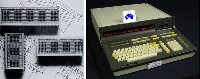 |
| The HP 5082-7100, First alpha-numeric display (on the left). It used a full 5 x 7 array of LED chips, requiring external strobing drivers. It came in 3, 4, and 5-digit clusters, which could be side-stacked for long lines. On the right, the HP 9830A, HP first personal computer, used the 7100 alpha-numeric display for direct dialog with the programmer. HP 9830A photo, Courtesy of hpmuseum.net |
The HP 7100 alpha-numeric display used a full 5 x 7 array of LED chips, requiring external strobing drivers. It came in 3, 4, and 5-digit clusters, which could be side-stacked for long lines |
One way to decrease the cost per digit was to share the driver circuitry. By clustering the LED character portion in a separate package and providing strobing driver circuits externally, we came up with the 5082-7100. An additional advantage was that we could feature the full 5 x 7 matrix of 35 die, which allowed for a very desirable alphanumeric display. Rolf Murchison was the key package and assembly process engineer for the 7100 and 7200 packages, later contributing significantly to our high reliability products.
The key early application of this alphanumeric capability was in the HP 9820-30 series desktop calculator being invented at the Loveland--later, the Fort Collins--Division. These calculators were powerful lab resources for computation right at the lab bench, rather than a time-share arrangement. Further, they were designed to be used to program and drive automated testing, by controlling a whole benchful of test instruments.
A variation of the 7100, full 5 x 7 die cluster, was a custom package we designed for our Santa Clara Division. They were creating a new HP 5300 frequency counter, intended for fully portable applications. As such it had to be battery operated, which immediately ruled out NIXIE tubes. It would always be a number-only display, which could be handled by a simpler 4 x 7 cluster of LED die. It confirmed the advantage of strobing with external driver circuits. By minimizing the die count, a very economical display could be realized. It became a very popular counter, in large part because the design concept included a variety of snap-on front-end signal processors. And the low voltage drive was perfectly adapted to a battery-operated counter.
|
|
More Information |
The 7200 was a 3-4-5 digit cluster of monolithic digits, packaged on ceramic, |
The 5082-7200 was a 1/10th inch high, monolithic display chip containing 7 segments that were mounted again in a ceramic package with a glass lid. The early GaAsP material was not transparent to its own light so down inside the crystal lattice, red light didn't transmit sideways. If you created multiple diode areas in a larger wafer, you could get a shape like a long segment to look very crisp, with no cross-talk or bleed-through between segments. The LEDs were very difficult to wire bond, very difficult to attach, and very expensive, particularly if you're doing multiple chips for a numeric display or for a multi character display. You have to have very high yields which means that you really want to keep things simple and low stress on the LED dice and wire bonds. That makes the multi-character production process more difficult, but the customers love it because they don't have to handle multiple tiny packages with all the data leads.
We Start Designing for Lower Cost to Remain Competitive
Now, interestingly enough, the Components Group was able to charge market prices for its products when it sold and transferred them inside the company. That was unusual because other inter-divisional materials transfers were typically valued at factory cost. However, HPA was not set up as a cost center to transfer at cost - it always had a unique status. This was a key part of the HPA success that HP -- which was a great customer -- was forced to pay market prices. Pretty good ones, of course, but we were allowed to sell on the open market. By far, our outside sales were much higher than internal transfers. The benefit to HP was that these high volumes accelerated our learning cycles and spread the overhead which lowered the overall cost and prices to the other HP divisions. I believe the competition of keeping our competitors out of HP instruments, of working with HP’s competitors, including Fluke and Tektronix, as well as having to find our own way in the open marketplace, made for a very competitive, very honest relationship with HP.
At times in later years, HP really wanted to revoke that charter, particularly when we were selling millions of optical shaft encoders to the printer division, and making, frankly, a very nice profit on that. But the constant criterion was, "Okay, you're not guaranteed any business from HP, they can buy from anybody, and you can sell to anybody as long as you don't violate confidentiality agreements, or get into a conflict of interest. And you sell at market rates all the way around, and you live or die based on whether or not you could make money." So that was a very good situation to avoid the classic problems of a start-up being absorbed by a larger company.
The market quickly told us that HP needed a lower cost numeric display than the 5082-7000. It wanted a product whose reliability was less military grade and more commercial, and far cheaper. The obvious question was, "Well, can we do this?" So, for my initial 7 months I was involved in solid-state displays and ICs. At that point, I had to take a six month leave for my National Guard training. I came back in late 1970 and, by that time, management had decided to delay the development of a cheaper solid-state numeric display each with an IC on board because a single off-board system IC was more cost effective for the customers.
We had very limited success with the 7200 as they were not end stackable without creating a larger space between the characters. With limited applications for 3, 4 or 5 character, one tenth of an inch high, displays and an expensive price point, it was more a novelty and a design/prototyping tool to get people to think about LED displays. We started the 7400 program to make a lower cost, plastic encapsulated version of the 7200 which would be end stackable. This project was already underway before the HP-35 project came along to hijack the project’s schedule and volume ramp.
|
|
The HP-35 Handheld Scientific Calculator and the 5082-7400
While we were actively inventing other commercial displays, we supplied a key component for the dramatic new idea of a handheld scientific calculator. John Minck covers the whole story well in his Narrative History, but suffice to say that we enjoyed our cooperation with the HP Labs team, and specifically Dave Cochran, who was responsible for the strobing concept, which saved power, and yielded display numerals which had identical brightness. Dave Cochran also wrote his HP Memoir, which is archived on this HPMemory.org website.
The built in magnifier lens was more sophisticated than it looks. We had to work with lens design programs to assure the look and feel of the final number display. We knew there would be an "egg-crate" effect, so the numbers looked a little like they were down inside an egg carton. We compromised with that effect and the desired need to have display images that were comfortable when someone was going to use the calculator for long periods.
The good news was that the HP-35 sales took off, going almost straight up. The story was that Hewlett had SRI run a marketing study to estimate what the monthly sales rate would be. The number came back at 500. Luckily, HPA management had concluded that no matter what the internal HP-35 demand would be, that we needed a HUGE facilities expansion, because we were planning on rapidly growing external markets to expand our production. We got a specific budget increase approved by Bill, based on his personal excitement with the calculator. But, honestly, we sandbagged him when Minck and Weindorf went to his office to get him to sign off on a substantial equipment and lab spending plan. And how lucky were we that we did that? Well, the HP-35 sales soon reached 10,000 per month. If we had not pre-planned that expansion, we could easily have turned out to be the roadblock to meeting the production demands.
One interesting story from the HP-35 calculator project is that we were developing a product that required a magnifying lens. Tom Whitney (calculator project leader), Barney Oliver, and Hewlett, decided that the display needed to be 1/8 inch high, so that it was easily read at arm length. But to use a full size monolithic character would have sucked about 50% more power, and cost a lot more too, because it required about 50% more surface wafer area. So we concluded that we could use a 1/10th inch high real digit and supply a magnifier over it.
The molded plastic part didn't have a flat top, it had a round magnifying shape over each of the monolithic LED chips, as we were creating a multiple character product to replace the product mentioned earlier, the 7200 display. The lens was to save money, because LED wafer area was very expensive - they really wanted to work with a smaller chip that would be magnified. HP thought that was too high-risk to depend upon -- for us to have an optical surface as part of a plastic part. So what they really wanted from us was just a flat, rectangular part that had the chips in. They still wanted the magnification, but they didn't want us to provide it.
They contracted with Optical Coating Labs (OLCI) up at Santa Rosa to create miniature Fresnel lenses. This was the same company that was making those 18 inch plastic Fresnel lenses that people would stick on back of car windows. They looked a little like a porthole, and when you looked through, you'd see a wide viewing angle. The idea was to create a miniature version of that with five 3/16th inch circles stacked next to each other. It was a little plastic strip that would go on top of the five character display, with no contact. That would go into the HP-35 calculator, which needed 15 characters, and you'd have three of these packages stacked end-to-end.
We participated in several visits to Optical Coating Labs. Then time went on and it became obvious they were overdue on providing working samples. Our project was hot, so along with Dave Cochran and some other guys from the HP-35 team--because I was at that time the coordinator for the display with the HP-35 team--I went up to Santa Rosa. The general manager came out and apologized and said, "I'm really sorry, I don't know how to tell you this, but my entire team quit last week. And in fact, they had been working on something totally different than your product, and they've made no progress on this." So HP Labs had no choice but to come back to us down at the division, actually the department at that time, and say, "You know, you talked about an integral cast epoxy lens, can you do that?" We said "Well, we're making progress." It will still have minuscule bubbles in it.
At that time, I was in R&D and working for Dick Soshea who was the R&D manager working on the program. We were trying to see if we could injection mold a plastic lens over the top of the 1/10th inch monolithic chips--because it would be much faster and get the bubbles out. Many Saturdays we worked on the molding experiments. We never could eliminate the bubbles so we went back to a casting technique, just like the individual lamps had used. We were able to meet the deadline for the HP-35 and the plastic 7400 series became a very successful program.
We worked continually with the calculator division team on new products and applications as they started up in Cupertino and then moved to Oregon. After the booming success of the HP-35, they soon started other more powerful and complex calculators for other purposes. There was the HP-65, programmable using a tiny magnetic card for storing and entering programs, the HP-55 that added features and registers while dropping the magnetic card feature, and a 35 upgrade, the HP-45 that added financial calculations. The first display products were on lead frames and then we moved to PC boards because we could get longer character strings for the full line, it was cheaper to make, faster to tool the constantly evolving variations, and it was a single drop-in for our customer. There was always a trade-off in terms of display cost versus viewing angle. Also as the junction gets smaller you get some favorable effects on current density. So the chip gets brighter and with the higher magnification you get more light out on axis but at a loss of viewing angle. There was a definite desire to minimize the size of the chip for cost and performance reasons, but yet you had to have good viewing angle.
I remember one time we had a meeting in Cupertino with Ralph Lee, who was Bill and Dave's EVP & Corporate Manufacturing Manager, and a pretty tough character - very demanding, very smart, very technically strong. He had walked by and looked at a new product, the new HP-4x Series calculator line that they were developing. He commented that, "Gee, this character looks kind of fuzzy, what's wrong with the character in this calculator display?" Such a pronouncement by a high level manager like Ralph creates all kinds of furor, people going back and looking at the optics and everything else. Finally someone decided to take this calculator apart and look at it, and there was a fingerprint smudge on the inside of the calculator’s lens that had created the problem.
The Monolithic product line expanded quickly as we sold to many calculator companies until LCDs took over.
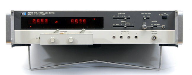 |
| The HP 4271B LCR Meter was an internal HP application for the 7300. It used 10 x 5082-7300, 4x7 array of LED chips, driven by an IC decoder on board. |
 |
|
5082-7300
Our answer to the cost issue of the single digit 7000, was to design a more economical array of die, with a 4 x 7 matrix, and since it was to be digital only with no alpha characters, it used only 20 die chips. The package had a ceramic base with interlayer wiring, thanks to the magic of Vic Wroobel's expertise with the technology of stacking green ceramic layers with internal wiring, and then firing them for the final rigid base. It used an on-board IC decoder, for the BCD data inputs. Vic also led the 7300 development program. Dick Kern managed the dot matrix display manufacturing lines.
 |
This clever design not only reduced the LED die count to 9 (2-dots), but featured an optical reflection method to stretch the illumination of one die to a full linear segment. |
In the quest to lower costs even further, the 7700 numeric family was based on optically stretching a small square LED into a long narrow segment by internal light reflections from a white TiO2 loaded plastic “light scrambler”. Commonly called the S4 family for Stretched, Strobe-able, Seven Segment. The epoxy filler was loaded with glass to improve the light uniformity and viewing angle with excellent resolution and brightness. The light scrambler concept was invented and patented by Roland Haitz, and copied by most of our competitors. It proved to be very valuable in trading for access to essential patents. By this time, the available colors included red, yellowish-green and yellow-amber, adding to the variety of applications. Seven segment formats were not very pleasing images, but the simplicity of circuitry and the low cost made them very appealing to the customer's design engineer. With our line of quality 5 x 7 fonts, as well as 7-segment, we had most applications covered by this time.
The 7600 and 7700 family also launched a variety of colors for the displays. This product expansion offered customer designers precisely what they needed to match their display application color format or brand color.
How to Design for Font Aesthetics
HP-35 display font: I got involved in the design discussions and actually created the original artwork - I cut the 100 X Rubylith original artwork for the monolithic chip that was used for the HP calculator, the 5082-7400 series. We had a lot of debate on the human factors of the font choice. Such discussions were frequent in the publishing industry, ever since the Guttenberg Press, with hundreds of years of styling and design preference discussions over printing fonts. Some of the same discussions took place in our engineering group. In a way, it seemed out of place.
For example, do you add a serif to the numeric edges, which stylizes the font? What is the advantage of making the two vertical sides of the digit with a slight "barrel" shape? If you do, the round characters like 0, 3, 6, 8 and 9 look better. But if it is too curved, then the digits 4 and 7 look odd. We did finally put a slight barreling in the shape, which did indeed make the digit appear softer. We tested many different shapes and tradeoffs, with our own staff, non-engineers, and industrial designers at HP, different ages for different eye skills, and what's the right character height versus cost? What's the right stroke width within the segment? How long do you make the different segments to create the most pleasing character? Does the center segment belong in the absolute vertical center or slightly higher? It would be too time consuming and costly to prototype all of the options as LEDs so we created photographic films of 15 random characters, back lit by a red light for the studies.
LEDs vs. LCDs for Calculators
The real problem with LED digits in hand calculators was that the LEDs took up too much power. This was crucial for a battery-operated product. But the fact was, that the original HP-35 design team, and Barney Oliver in particular, wanted to go with liquid crystal displays (LCD) in their first design. But several limitations hit them head on, first, they were too unreliable at that point. And second, the HP-35 needed 15 digits, in order to display the 10 significant digits and exponents in base 10 scientific notation along with signs. LCD display pixel resolution produced fonts that were too large to fit 15 digits into about 2.5 inches. Now, of course, all cell phones do that.
LCDs were already starting to appear at that time, such as in some watches, but they hadn't worked out. The reliability issues for LCDs were many, how to prevent damage from the strong UV rays, on a wrist. Or UV damage that occurred just being in a storefront window which caused serious degradation in contrast. The lifetime of the organic material of those years was even more serious. These were made with about 10 thousandths thick layer of compound, sandwiched between two glass plates, with tiny numerically-shaped electrodes on them. Then the two glass plates had to be hermetically sealed some way. It was hard to do with a hot flame, because the organic liquid was damaged from the flame.
But epoxy sealants weren't perfect. The packages leaked. Trying to maintain a seal over that much glass was very difficult. So when they started the HP 35 program, they took their second choice, and ended up going with LEDs, knowing that in the longer term, the LCDs were a better source. Hard as may seem to believe, it also happened that the organic compound would develop an "infection" from impurities or leaks. The infection would start on one corner of the display and slowly just creep over the whole surface and disable any characters.
LCDs were excellent in direct sunlight, because they depended on light reflection, while the LEDs active red light had to compete with the sun. We called that washout, and it was a serious deficiency for some applications, like airplane cockpits. For dark conditions, LCDs needed a backlight since they didn't have an active source on their own. The LEDs consumed too much power, and the LCDs were very low power. So it was only a matter of time before the LCD technology, once they became reliable enough, became the preferred display technology. Further, as the displays were required to present more data information, it became very difficult to do that with individual LEDs. To get a string of 50 characters, it would become quite easy with a single LCD glass area, as witnessed by even the cheapest cell phone of today.
Within a few years LCDs completely replaced LEDs (in calculators). So we weren't really supplying anything to the HP calculator people, other than maybe the occasional lamps. We were supplying numeric displays and alphanumeric displays to the instrument divisions. But, the slumping shipments of LEDs to HP was replaced by our supplying the optical shaft encoders to the inkjet printers and X-Y plotters. Soon all the plotters were replaced by ordinary printers inside HP. At the time of the Agilent split, we were doing a huge amount of business supplying, sole source, to HP for its optical encoding needs.
Management
Some of the LED display department history is recorded in Minck's memoir, since he spent 3 years getting it going. John had been Microwave Division Marketing Manager for 6 years before his move to find a more technical assignment for a time. I think John Young wanted Minck down to HPA because Young recognized that HP corporate was going to be a big user of LED displays, and that the HPA components people needed someone who understood the needs of their traditional measurement company product line. And that's how it worked out, since we nailed a number of key instrument display applications, including the blockbuster HP-35.
By the time I was hired, Dave Weindorf was HPA Division Manager. He had succeeded Don Smith, who had joined Melchor in venture capital work. The early engineers working in the display department were: Vic Wroobel, an expert in ceramics; Rolf Murchison, package and assembly engineering; Joe Diesel, handling test fixturing, software and production testers; and Hermann Luchinger, wafer fab engineering, running the epitaxial furnaces. Howard Borden was my boss, and was in charge of product engineering. His early work was in some of the earliest silicon startups in the Valley, at several semiconductor companies like Rheem and General Microelectronics.
Jack Melchor was never in active management at HPA, he was an investor only, although his technical expertise was occasionally called on. He was close to other HP corporate managers. When John moved to HPA in 1969, Gerry Pighini moved out to Fairchild, to join his poker-playing buddy, John Attalla, who had been hired by Fairchild to build an LED operation there in their R&D headquarters behind the Palo Alto Veterans hospital. John went out and hired Roger Likens, an experienced production manager from Fairchild in Mountain View.
Marketing was not attached to the LED Department, but reported to Milt Liebhaber, HPA Marketing Manager. Rick Kniss was Display Marketing Product Manager. Reporting to Milt, Jim Girand and Pete Manno were in the sales department, which handled the entire division line, microwave as well as LEDs.
In 1972, when Minck moved back to the instrument side of HP, Paul Gallagher initially replaced John, for maybe 9 months. But the real key to the long term success of HP LEDs was that Bob Zettler returned from Fairchild MOD group, (their microwave and optoelectronics group), to head up our Display Department. He'd been there, along with Paul Sedlewicz, working on microwave diodes. If anyone can be given credit for the early success of the HPA optoelectronics activity, it was Bob Zettler. He brought in operations understanding, as well as a technical comprehension of how to lead in semiconductors processing. He was certainly strong technically. He was very detail oriented, with incredibly good business sense, and an amazing memory for details. He energized the whole department. As we grew and became a new division, he was the obvious choice for our Optoelectronics Division General Manager.
With sales growth, the division split as we developed both "non-visible" and visible products. Examples of the non-visible were infra-red emitters and detectors, and high speed optical isolator products. In the 70’s that product line split off as a different division called the Optical Communications Division under Dick Soshea. Dick Soshea had headed up Opto R&D, which was also external to the Display Department., and was replaced by Roland Haitz, who had joined the opto activity in early 1970, coming from TI. Dick left in the mid 70s. Bob Zettler continued his role as general manager of the visible side, which continued to be called the Optoelectronics Division, and oversaw rapid growth due to popular display products and competitive prices.
Meeting Customers at Home
When I came back from my military active duty, my first task was to define the driver logic for the strobing principle of the horizontal and vertical scans of the 5082-7100 alphanumeric cluster. This was a 1/4th inch high character, which was selected for the most powerful of the HP 9820 and 30 Desktop Calculators at Loveland. These featured software programming, via their keyboards, and since they didn't use a CRT display, the 7100 was ideal. The 5-digit clusters could be stacked end to end to make a long line and pleasing readout.
A 1975, HP Optoelectronics Product Selection Guide |
Following that strobing application, Bill Hewlett’s personal project, the HP-35, began to take my time in assisting Dave Cochran, the algorithm guru. He was also responsible for the strobing technique of the monolithic display of 15 digits. After that, I went into applications while continuing to design decoder and driver circuits. Hans Sorenson was the application engineer for the opto-isolators, and I was the application engineer for visible optoelectronics. Key technician support was provided by George Liu and Al Petrocello. In 1972, Hans and I presented papers at a Swiss conference and then spent several weeks traveling around Europe to train customers on optoelectronics - what were LEDs and how to use them in a variety of common applications. This was the first time I was able to go out and see real customers.
In 1973 we also took several one and two-week trips around the U.S., giving application seminars to customers. On-going customer seminars were enabled as I added Dave Evans, Mark Hodapp and Stan Gage to the applications team. These seminars set the precedent of HP Opto being at the technical forefront of not only products, but also customer engagement. This approach was key to our market penetration as few of the potential users knew about LEDs, their advantages and how to use them to advantage. These presentations formed the core of a soft cover applications book that would spin off a number of application notes. Years later the applications team under Stan Gage would author the essential technical optoelectronics hard cover book, published by McGraw-Hill.
Jumping into the Deep End in Manufacturing Management
Wanting to broaden my experience base, I transferred in the late 70s to Manufacturing as the Engineering Manager of the Monolithic and soon to be S4 display product lines, reporting to Norm Tarowsky, the Product Line Manager. Manufacturing did a lot of the non-breakthrough product development (product proliferations), as well as run production. The Manufacturing Product Line Managers were the defacto business managers. When Norm moved to Singapore to head up the Asia Manufacturing Operations for HP Components, I took on his role as PLM. In truth, at that time I was poorly prepared for the business side and busied myself with the technical and production challenges. The management environment was to throw you into the deep end without a life jacket.
When an opening appeared in the early 80’s to manage OED’s Palo Alto Instrumentation Development Group, I transferred – Norm Zinker was my manager. The demands for high volume quantitative testing of color required a never before possible tester concept. Previously, operators would manually bin the different shades of a color using limit samples for each product category (as with light flux, the chip and packaging process variations produced a wide shade range of colors that if combined were objectionable to the eye). The Instrumentation team, led by Steve Waisner, had demonstrated a solution but we needed to sell it to Jim Leising in Manufacturing before it could be implemented. The task fell to me. While Jim was skeptical, I was able to explain the science and, more importantly, convince him that this would give a production worthy solution - that our team could deliver and support the machines for production in Singapore and Penang, as well as Palo Alto.
Thus was born the very successful line of ET10763 testers which were a staple for over a decade. In fact, a number of specialized testers were developed over the years.
Finding My Home in Product Development, circa 1981
After 3 years leading the test development team, I moved to Product Development as a Section Manager reporting to Stan Gage who was now the OED Product Development Manager for Visible Products. Moving beyond numeric products, we were expanding our on-board IC products into the alphanumeric realm which required custom ASIC ICs for data management, decoding, and constant current drive of the LED diodes. Litronix (later Siemens Opto and later still Osram) was our key competitor. We developed and second sourced a number of 4 character 14 and 16 segment alphanumeric display products. This led in the late 1980’s to developing custom displays for the new industry leading Star Tac line of Motorola cell phones.
As color LCD displays were not yet reliable or cost effective, the Motorola VP (Wiseapple) decided to differentiate his products with LED alphanumeric displays. They continued to get more complex, ending up with 2 lines of 7characters on a single high temp pc board substrate requiring 500 LED dice and 4 custom ASICs. Tom Lugaresi and Akhtar Khan created the ICs while Shane Harrah and Mike Lam developed the package solutions. By using existing die attach and wire bond processing, our schedules, performance, yields, and costs met our targets. Volume ramps were extreme and unpredictable, as you can imagine for this product that was the darling of the mobile phone business. We had joint technology road map reviews with the Motorola technical management to coordinate the solutions. This business exceeded $60M for OED at its peak and was jointly managed as a business unit by Aneta Davis (Marketing Section Mgr), Bill Beecher (Manufacturing Section Mgr), and me leading the Product Development section.
Annual five year business plans were generated, and kept current. After several years of success, it became clear that color LCDs would take over the business from LEDs and margins would become unacceptable. Bill, Aneta and I recommended pulling the plug on new Motorola business, leaving the field to Litronix. Our managers agreed. Managers from Litronix later told us we got out at the perfect time. Shortly after our exit, Motorola replaced Wiseapple. With the champion for LEDs gone, new phones switched to LCDs as used by the rest of the industry. Note this activity overlapped with my on-going work with optical encoders, which is described below, and which ran on for 16 years from ~ 1983 to 1999.
The HEDS-9000 optical shaft encoder was a marvel of accurate performance as well as production automation. |
Optical encoders are a major tool for motion control using optical feedback. An optical shaft encoder is very simple in concept - you take a round disk and etch radial slots in the outer region. You place an LED light source on one side, and an IC with a silicon area that senses light on the other side. As the disk with slots moves, it will break that photon path to prevent the light from hitting the detector. Optical sensors using LEDs and photo detectors have been around for a long time, even going back to the early days when I first joined HPA.
What is new is that HP Labs created the concept of an innovative rotary disk and paired emitter/detectors, which worked through axial slits, to sense a rotary mechanical motion with extreme precision. It just didn't detect whether the light was on or off, but it would detect and decode a whole array of on-off cycles coming off the code wheel. The fundamental encoder development work and key IP was done in the late 70s and early 80s in HP Labs and OED by Jim Cascani, Mark Leonard, Howard (Tsvi) Epstein, and John Uebbing. It used a varied pattern of 10 stripes of light that were impinging on 10 alternating stripes of a detector. With these position-scanning techniques, we were able to intelligently tell the speed of the code wheel and its direction with high precision. It was first used to control the horizontal movement of the ink carriage going across the paper. See the initial HP Journal article of 1981. This project was transferred to HPA Division to complete the development and proliferate as the Scorpion and Turtle products. Manufacturing was led by Bill Beecher at the old Palo Alto Harbor site. While a breakthrough, each encoder required an adjustment at final test to optimize the position of the separate phase plate.
Up until that time, people had been using stepper motors, or other open loop control systems, to position the printer ink head, and tell the printer where it had to go. But it didn't really know how far it had actually gone, and therefore it was limited in how fast it could go, so its resolution, repeatability and accuracy were crude. These optical coders that we provided were really a breakthrough in the business, because of the strong patent position we enjoyed. It was a key part to HP's success at creating breakthrough print quality and print speed .
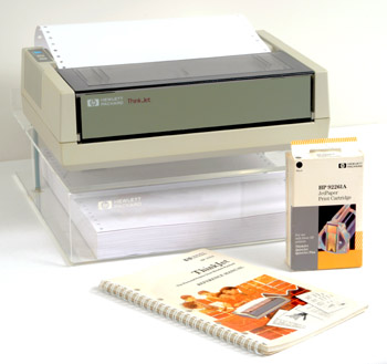 |
The HP 2225 "ThinkJet" Printer, only one font, no graphics, special accordion-fold paper, but customers loved it. It launched a dynasty. |
HP was one of the first printer manufacturers to use electronic control with closed loop feedback for controlling the print head in its horizontal path. It was a very large and very successful business for HP, and we were part of that. We were there from literally the first days of the ink jet printer: the HP2225, a little magical box that used special accordion-fold paper, which customers were willing to tolerate to get page printout, characters only, no graphics at first.
Before our move from Palo Alto to San Jose around 1983, Stan asked me to manage the development of motion control, optical encoder products, starting with the breakthrough Zipper product. The Zipper program would change the face of optical encoding and close loop control by redesigning the Scorpion and Turtle products for high volume, low cost, and high yields. By integrating the phase plate into the IC, the tuning process at final test was eliminated. Insert molding around a lead frame provided both the substrate and output pins, designed by Chris Togami. Working with Manufacturing engineers (Larry McColloch and Victor Loewn who were led by the engineering manager, Bill Loesch) the assembly process was made robust. Rob Nicol was a development engineer who transferred into Manufacturing with the product transfer. Bill Bilobran contributed key test software. A Kanban type, pull line was set up by Larry McColloch in San Jose that eliminated rework, assured optimal levels of work in process, and prompt feedback of any yield issues. After running in San Jose for a year, the lines were transferred to Singapore due to the exploding volumes. Dual-degreed in ME and EE, Larry was known for his automation equipment with craftsman quality, stained fine wood front panels – works of art. It hurt him deeply when Singapore later painted them all the line’s standard “Toshiba” white.
The Zipper was designed into a line of pen plotters for San Diego Division. This decision attracted the attention of the Vancouver Inkjet Printer Division, however, they needed a lower cost encoder and promised extremely high volumes. Redesigning Zipper for still lower cost and very high volume became a joint project between Product Development and San Jose Manufacturing. Chris Togami was the key package designer for the Zipper II project. Different applications required different mounting profiles, such as detecting encoding stripes on a long horizontal strip or a rotating vertical disc. Rather than redesign the basic package, Richard Ruh provided the idea to create individual mounting clips that would all use the same basic “engine.” The clips were just simple plastic and easy to mold, allowing the production line to build one standard encoder for a variety of applications. Since applying the clip was the last assembly step, changes in build mix could be easily accommodated. See the follow-up HP Journal article on Zipper II by Epstein, Leonard and Rob Nicol in 1986.
The diagram below shows the clever design-for-manufacturing concept. The insert molded, stamped leadframe came in a strip of approximately 6 packages. The frame was its own production carrier. That's the state where all the die attach, wire bonding, IC cover and lens insertion was done. All stations ahead of Trim and Form were linked for fast cycle time. The final step before test was a Trim and Form tool, which punched out the tiny connecting webs and folded the flat part into a U shape. This then fed into a final tester.
We mandated there would be no rework, and used Kanban production control to limit the Work In Process, so that any yield abnormalities at final test were quickly fed back to the line. Cumulative yields for Zipper and Zipper II were always in the high 90's, which resulted in low costs, predictable shipments, and the ability to quickly respond to order volatility. That was crucial, given the large variety of codewheel format counts.
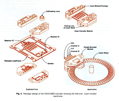 |
| Expecting production volumes of hundreds of thousands, the mechanical designers came up with a clever folded assembly, which fit well with production automation. Note that the upper right image gets folded, to result in the final installed configuration. |
Around this time, Jim Leising took over from Stan Gage as Product Development Manager when Stan followed Mike Cowley up to Corporate Quality. Jim had been our wafer fab engineering manager. HP believed in promotion from within and this was one of many examples which gave continuity and breadth as managers came from different departments/areas. It certainly was true in my career where I moved between development, technical customer support (usually a Marketing function), manufacturing, technical service groups, product development, and worldwide program management. Jim Leising is an incredibly effective manager and leader, as well as a great technical problem solver. He was my best manager over the 43 years and a career long mentor. I'll always appreciate how he helped me grow in my career. He later moved up to be the Strategic Merger and Acquisition Manager for the HP Components Group.
At the time that Agilent spun off from HP in 2000, the Inkjet Printer Division had added a second optical encoder to control the paper position and speed up the vertical paper motion. The reason was that inkjet printers had new software which did graphics, not just lines of type. For that function, you now have to position, both in the x and y directions very accurately without sacrificing speed.
Using the key encoder IP, an extremely profitable business was started, which continues today. A management team, similar to the display business described above, ran Motion Control until it was transferred intact to Singapore in 1999. Karen Owyeung was the Marketing Section Mgr (later replaced by Chris James as she climbed the management ladder), Bill Beecher led Motion Control Manufacturing, and I had the Product Development Section. We formed a close working team and created a highly motivated cross functional team of engineers and technicians. Through extensive domestic and international joint travel, our business management team formed a close relationship with our extensive list of consumer and industrial customers, many of whom were competitors (e.g., HP, Epson, Lexmark, and Canon). At one point, Motion Control was so profitable, it subsidized the division. The 3 sections functioned as a seamless team, solving the problems and creating the many successful products. I led the development of our motion control products for 16 years. It was the most successful and personally satisfying experience of my career.
I move out of LEDs
With the Motorola development at an end, future display development moved to Manufacturing in the mid 90s. When Motion Control’s Marketing, Manufacturing support, and Product Development was transferred to Singapore and Penang in 1999, I led the transfer and joined a worldwide tour of our key customers to introduce the new management team and pass the baton. I turned off the Motion Control lights in San Jose in 1999 after spending 30 years with visible OED products. So, time to find a new challenge. Ram Krishnan had been one of my project leaders and most recently a business manager in OED Marketing. With the rise of fiber optic telecommunications worldwide in the late 90’s, this area of HP’s Optical Communications Division was exploding. Ram had transferred to the OCD Marketing department in late 98 or early 99. Knowing that my current job was disappearing, Ram suggested that I apply to Fiber Optic Product Development. The R&D Manager, Ron Kaneshiro, agreed, and I became the section manager for Storage Area Network devices, a new area of focus and high growth for customers like Cisco, Brocade, and Juniper. With fiber optics, the main limitation to data rates was the transceiver that handled the electronic signal to light translations and back. A new 2 GHz transceiver platform, Dos Equis, was the next breakthrough assignment. Pete Mahowald was the project leader. Various proliferations followed.
A Sad Experience as We Lose the HP Name
Dad's company was a member of the Western Electronics Manufacturing Association. WEMA, which changed its name to the American Electronics Association, later merged with the Information Technology Association to form TechAmerica, a trade group, actually was started by Dave Packard and other owners. So at dinner meetings and conferences, dad would run into Bill and Dave, and say “Hi”, no business dealings as they were in different parts of the electronics business. But he was always impressed with those men. And they were a culture in the Valley, for anybody who had grown up here. Later, of course, they became a global culture beyond that. So when you said that you worked for HP, there was this incredible pride that came through, and recognition by others of, "Wow, that's a good company, and they hire top people."
So I felt a great sadness at losing that association when we were spun off as Agilent. The new Agilent CEO, Ned Barnholt, tried to recreate that company culture and that old instrumentation spirit. At the time we felt that we were getting the best part of the HP products, and certainly the best culture because we could see the culture already being sacrificed at HP for the sake of the IBM-like computer business and the consumer marketplace of PCs and printers. We were the ones holding on to the values, but we lost the bragging rights to say that we were HP employees.
My Trail to Lumileds
It didn't bother most people at the beginning, but there was a great business bubble within fiber optics telecommunications in the late 1990s. Recall that first round of Internet companies like Webvan, the grocery delivery startup, and others? There was plenty of venture capital, chasing ideas that just weren't economically viable. John Minck also told me that was the period when the fiber infrastructure was riding that boom too. They dug up El Camino for miles around Palo Alto, cementing in conduits of hundreds of fibers which featured 4 manholes every 300 feet or so. He said that one of his friends told him that 90% of those fibers pulled into the ground were dark--no traffic. It would take 10 years to load them with traffic.
So the fiber optic telecommunications bubble was huge everywhere, and we rode it. We were extremely profitable, and then it collapsed back down. Agilent had to basically stem the bleeding, and so that was what was done. Agilent came into the separation period from HP accepting too many people in the split, partly because they showed a huge order backlog. But as usual, many of those apparent backlogs consisted of double ordering to assure deliveries. Bad idea.
When the bust came, all of the suppliers were affected as well as the telecommunication companies. After being with HP and Agilent for 33 years, in 2002 I was laid off. They eliminated my part of the management structure - that was tough for me to take after growing up with the HP family; like someone had died. Eventually over 50% of our San Jose division was laid off over a period of five different layoffs. Agilent, like HP, offered a very good severance package. They gave me two weeks to find a job inside the company. After a week, it looked like they might be able to create something for me, but I didn't think it was last long and I believed that there would be other layoffs in the near future.
Jim Leising took over Product Development from Stan Gage and had been my manager in OED R&D for a number of years. Jim is an excellent manager and a great guy - the best mentor of my career. When I was laid off, Jim was in a high level staff position at that time, doing strategic acquisitions for the Components Group. Jim put the word out to Lumileds that I would be a great hire. The Lumileds management knew me since I had worked in the same building with all the Lumileds people over the years. At the time Lumileds was started, I was not in the lamp side of OED – I was in the Motion Control. So my great story was, that after a week when I didn't see anything happening on the Agilent side, I walked over to the other building, and in 24 hours I had a job. They didn't have a current opening, but made one for me. Only in Silicon Valley – moved companies but kept the same phone number and used the same driveway.
Lumileds’ offer was for an assignment in Frank Steranka’s R&D department. They told me they weren't sure what I would do: "We have confidence in you and we'll find something for you." Now THAT is a nice feeling, just having been hit in the face with a layoff. So I took two weeks off, and when I came back they said, "We have a collection of projects that are all leading to reinventing the current standard Luxeon platform for the illumination business. We want you to lead that program. The world has really gone to surface mounting. However, Luxeon was invented six years ago and will not survive the reflow solder process of surface mounting.” Luxeon didn't meet current normal industry standard processes, and needed serious redesign.
So, I led the R&D Section with responsibility for our next major lighting platform. This was the Luxeon K2 (named after K2, the most difficult mountain in the world to climb, because of the large number of challenging requirements we faced). The lesson learned was that just because Marketing and management want to simultaneously do 5 world class breakthrough requirements and multi-source all your custom parts, you can create a “bridge too far”. While it took us significantly longer than planned to develop the K2, it was a true world class, breakthrough product earning the industry’s Worldwide Product of the Year Award. The key designer was Fernando Teixeira with thermal analysis/design by Frank Wall. Work then turned to proliferating the platform family.
The Evolution of Power Illumination
The question was one of improving cost and efficiency, and finding a market match. In the mid 90’s we started to see the opportunity for rear lighting on cars with the new requirement for a Center High Mounted Stop Light. We didn't think about forward lighting at the time, because the idea of a phosphor converted white light product, which is now pretty commonplace, hadn't really appeared. The idea of trying to use red, blue, and green to somehow make a bright-enough and cost effective head lamp was beyond the then current technology. But then the first white lamp process came along. The breakthrough, by Nichia, was to use a deep blue emitter to pump photon energy into a particular phosphor whose yellow light combined with the LED’s blue light to create a white light. Being part of Philips, the potential for high flux emitters in illumination applications was clear to Lumileds at its beginning in ’99.
 |
So Lumileds started a new direction for LEDs by designing LED chips and packages for higher drive current, higher light flux levels, and greater heat dissipation. This was the genesis of the Power LED. The analogy I use is that transistors started with the very small TO-92 transistor - a small signal transistor, low power package not intended for high power applications -very similar to the early 5mm diameter LED lamp. With the increasing power requirements for transistors, the industry created the breakthrough TO-220 package with a big metal heat slug for reliable dissipation, sturdy leads and robust packaging. That's what Lumileds did with its light products, particularly the Luxeon emitter. It was a product entirely developed for high volume, high power illumination type businesses. Luxeon was the brilliant vision of the future. And Lumileds had that vision when it first started.
Lumileds first started as a joint venture. But my understanding is that Philips approached Agilent, actually HP, since this happened some time before the Agilent spin-off. They brought their vision of what could be accomplished by focusing on power LEDs as a light source. It was an obvious win-win; Philips is one of the top three lighting manufacturers in the world. It’s unclear to me whether this was a pre-emptive move based on a belief in this future technology or a defensive move to counter a potential move by one of their competitors. They certainly were considering all threats to their then dominant technologies. I suspect their action was at least as much a threat response as an understanding of the technology’s potential. So Philips approached HP and worked out a deal where they each put an equal amount of investment into the game – for HP it was primarily the people, facilities, and certainly its considerable patents; while Philips brought the money, it's expertise in illumination systems, and obviously, its brand identification with the marketing channel and their customers in the illumination business.
When I joined Lumileds in 2002, it was clear to me that, strategically, Lumileds was strongly aligned with Philips, and the Luxeon product was something that was going to be very useful for them. It wasn't going to be useful for HP or Agilent. To me, it was only a matter of time before the parents agreed on how Philips was going to buy out the other half. Certainly it was a big kudo to Lumiled's employees, to realize that we were now valued by the market at $2 billion, because Philips paid $1 billion for the second half. The transition of systems and culture was done gradually, a smart move by Philips given that Philips had lost its appetite for risk and innovation. Unlike its early years when Philips’ innovations were legend.
Back to Test Development
Following completion of the K2 product development program and its proliferations, I was asked to lead Product Development’s Test Development Section in San Jose. This group had worldwide responsibility to provide test solutions for new product platforms and performance capabilities. A key activity was to coordinate with my test manager counterparts in our Manufacturing locations in Penang (Malaysia) and Singapore. First of its kind activities for Lumileds included quarterly worldwide test summits and test development roadmaps that aligned with our product and performance strategic goals. One highlight was the development and implementation into high volume use of the world's first "hot LED test" where 100% of the products are fully tested for all guaranteed electrical and optical data sheet parameters at production test rates at elevated temperatures, allowing the data sheet to actually spec the part at the point it is used rather than at 25 degree C. This set the industry standard and within 12 months, all major LED manufacturers had implemented 100% hot, at use condition, production testing. Another activity was a significant increase in the tester repeatability and accuracy for flux and color measurements as required by the emerging Illumination market.
Worldwide Program Management for New Product Platforms
In February 2012, Lumileds management decided to create a worldwide test management position in San Jose with responsibility for both the Penang and Singapore test groups. However, my SJ management position would be eliminated. The WW position required extended visits to Penang and Singapore which was incompatible with my family responsibilities. I did not apply for the WW Test Manager spot and requested a lateral transfer to be a Director of Integral Programs. This is basically a non supervising position as a Program Manager with WW responsibility for the development of major new product platforms. I picked up program management for the new LED component that was incorporated into Philips Hue Bulb, released initially through Apple stores.
Lumileds' Work Culture (before Philips)
And what of the HP culture remains in Lumileds? One of the things that I tell people is that unfortunately we don't have the donuts every morning, which is better for my waistline. That was such a great HP tradition. We actually took the time to have a coffee break, and have the free donuts. Within a few years, unfortunately, the work pace picked up, and so people tended to grab the donut, walk back to their desk and keep working. That was unfortunate, and defeated the original purpose for it to be a true break and opportunity for networking.
One of the things that I tell people is that the one thing that I loved about coming to Lumileds, more so than any other organization, is that this company had a great spirit – an intense cross functional passion for our work. Despite its rapid growth, it had the aggressiveness of the early HP Components Group. The Component Group's culture was always a little different than for HP instruments groups. Components Group and then later the Advanced Products (aka Calculator) Group always were more aggressive, less tolerant, faster paced; and we worked longer hours than the instrumentation groups (at least my perception after visiting the other sites). But that was always under girded by the basic HP values. That never was sacrificed.
I think early Lumileds was a very well run organization - management was very much in touch with what was going on. We were constantly focused on and had a clear view of what our contribution was, what our business strategy was - creating business successes from breakthrough products. The Lumileds motto was "Never before possible".
So I think the classic HP culture was definitely here in the early stage of Lumileds. But better in a way because one of the classic things that came out usually in the open line surveys at HP and Agilent was that management was too tolerant of poor performers. That was probably the weakest part of HP; that it was so facilitative and so supportive of employees that I don't think management spent enough time resolving poor performance problems – coach the employee to improve; if they don’t, let them go.
Lumileds does not have that problem. As a company, we demand high performance. We were a very fair company. If a person did not work out, we would try and find them another spot. If that's not going to work out, they're not with the company anymore – quickly and quietly. As a result, there was high morale here because everyone had a lot of confidence in the organization and the staff. It was a good place to work.
Unfortunately, as Lumileds the start-up JV gets absorbed into the Philips structure, the passion is less and the loyalty gone due to the periodic layoffs and a larger structure.
Into Retirement
Judy and I decided that I would retire when I turned 67 in April 2013. In October 2012, when my manager was starting to plan the Program Management assignments for all of 2013, I gave 6 months notice of my retirement. So, on April 1, 2013 I retired from Lumileds after 43+ years with the same organization, although the company names went from HP to Agilent, to Lumileds JV, and a wholly owned subsidiary of Philips Lighting.
In retirement, I have left the work world behind with no interest in consulting or part time work. Our kids and grandkids live within 10 minutes of us - Chad with wife Liz and sons Peter at 8 and Ben at 6; and Erin with husband Courtney and daughters Hannah at 6 and Abby at 4. So lots of family time in addition to frequent travel, lunches and hikes with friends, and volunteer activities. And just taking time to do whatever we want without the need to rush.
Looking Back
I often think to myself when I wax philosophical, what were we ever dreaming about in 1969 - whether LEDs would turn into the HUGE business opportunity that they have? Did we ever envision how far it might go or whether we somehow saw what the future actually brought? And the answer is “Yes, in general but not the specific areas beyond a few years ahead. In 1969 we never thought of LEDs as being in the illumination business. Nor did we see it being so pervasive in terms of information display. We could see the large potential with the lamp; we could see it as the replacement of the NIXIE tube. We knew that success required development of both the product packaging and the LED material. You had to look for the opportunities and be agile in responding to the good and bad surprises.
HP became the only surviving major U.S. supplier of that LED processing technology within a few years. TI, Fairchild, and a lot of smaller companies fell by the wayside. Again, Bob Zettler was one of the real, the key managers who made us a successful HUGE volume supplier. He took us from a kind of a science curiosity, to making parts in high volume, that were reliable and cost effective and that were well marketed, and backed up with knowledgeable sales and applications staffs.
Rick Kniss was the key guy on the marketing side. Rick actually wrote the original business plan for the HP-35 calculator display. That was a blockbuster, in a serious way; it brought HPA out of the 1972 business recession. Then I could see it happening again, as we got into opening up the automobile illumination market. First we provided the third brake light for cars. We could start to see the future of exterior lighting for cars because of its reliability. And it provides a lot of styling opportunities for the auto guys, which is always important in terms of selling cars.
An observation on the transition from HP to Philips. It's great to be in a company where lighting is a core competence and key to their corporate strategy, instead of being a leftover from a time when the parent couldn't source their LED needs externally. However, Philips is a large and bureaucratic organization that is struggling to not smother innovation while it manages both old mature and new start-up organizations using the same rules and tools. Not a new phenomena. Gone also is the strong sense of company or employee loyalty at Lumileds as people don't stay long and major layoffs occur every 3-4 years. Again, a reflection of the time. This experience reinforces the very special nature of HP and HP Opto in the 70s and 80s. A privilege and a blessing to participate over these formative years for LEDs - to see firsthand the incubation, development, and mass adoption of not just a new technology but one that is making a very large and positive impact on our world.
I feel a keen sense of satisfaction that I was present and contributed to two significant turning points in HP's history. Number one, was the HP-35 calculator. When I came back from military leave, in late 1969, we had just started up this plastic version of the 7200. Technical discussions already underway with HP. And so I had a chance to work with three exceptional engineers. Tom Whitney was the HP-35 project manager, Dave Cochran was the genius who packed all of those computational algorithms into a relative small IC memory, and Bernie Musch. I was based down at 640 Page Mill Road, and so we would go up to the labs from time to time and work with those guys.
The second turning point was the HP inkjet printers and the use of optical shaft encoders to improve ink position and print speed. I spent 16 years in development of optical encoders and had a chance to work with a lot of people in Vancouver on printer designs, as well as with their competitors such as Epson, Canon, IBM and Lexmark. The worldwide cross-functional motion control team functioned as a pure start-up, seamlessly designing, creating, and delivering world-class, breakthrough products with outstanding revenues and profits, not to mention our great morale and passion.
Some Bill, Dave, John, and Lew Stories
Of course Bill's classic walking through the lab and checking the calculator models and whether they fit in his pocket, those were all true. One story that didn't happen to me, but it happened nearby and I know the guy who it happened to. We would have annual reviews, on-site business reviews with Bill and Dave, and they would come down and sit with us as the managers. And all the stories that you hear about Bill and Dave and their ability to question and probe are amazingly true in terms of being able to get to the heart of things.
But a classic Dave story is the first of two - there was a break in the middle of a management review. Of course, everyone runs out for a smoke break at that time or a bathroom break, and this was done in the basement in building 11. And right across from the major conference room in building 11 lower were a couple of small rooms with windows in the front. And while all the managers basically went out to get a coffee and go to the bathroom and grab a smoke, Dave saw there was a meeting going on in the next room with a bunch of operators that were in white lab coats. Bill Beecher was the Quality manager leading the meeting.
Bill loves to tell the story that Dave knocked on the door, asked if he could come in. He introduced himself, why he was there, and asked them what they were doing. And so they talked about what they were doing, and he was very supportive and he went around shaking everybody's hand and he left. Five minutes. It made a difference. So I think Bill and Dave have always been very supportive that way. They were really interested in wanting to do product fairs. And they would come through and talk to you -- whether it was going through the lab or there were poster sessions -- always asking very interesting questions about what was going on.
When John Young came through, he would ask questions, but John was the guy who was more marketing related. John gave you the impression that he was doing it because he had to do it. And he was just kind of going from step to step and asking questions, kind of like, a royal touching base, and then just could get on to what he really wanted to do.
I've been told by a friend that she met John Young once at the HP Addison Avenue, 50-year garage rededication. She noted that unless she'd known him in advance, she wouldn't have found out who he was. He was so low key, and was very quiet that day, since the ceremony was about Bill and Dave. John had moved into the upper management group in the early 1960s, when Barney, Dave, and Bill decided that they'd kind of messed up, in not bringing enough younger people into management soon enough, there was no succession plan. They went to the business schools. These were all guys who typically had BSEE degrees, plus had their MBAs, mostly from Stanford and Harvard. So there was a cohort of new MBA hires around 1958, that they brought in, and mentored and trained in the right culture. John was one of them. And John looked the part, he looked like a CEO. And that group, they called it “the class of '58, the group that the stars fell on”.
The second story is more personal. It was before I joined the fiber optics group, and certainly before the split with Agilent. So Bill and Dave were on site, in the Bldg 91. And I honestly don't know why, but Dave was just walking around, and seeing what was going on. People would start flocking around him and shaking hands, including me. This was in the mid 90’s, so he was long out of active management. Bill was in a wheelchair at the time. He didn't come upstairs. But he was talking to the advanced R&D guys on what was going on. They were both just such very personable people.
Another top manager I met several times was CEO Lew Platt. Lew spoke at Dave's memorial, and he spoke I think for all of us, that Dave was most people's "closest personal brush with greatness." I had a chance to spend a morning with Lew Platt in a jury pool room. It turns out we were in the same jury pool, along with Gary Baldwin who was a lab manager at HP Labs and HP’s campus manager for engineer recruiting at Berkeley. I got to know Gary because for many years I was on the Berkeley recruiting team, at the invitation of Bill Craven, our Group GM who was an active Cal booster and alum. This made for some interesting conversation when the students asked if I was a Cal grad.
I was standing in line waiting to check into the San Jose's Superior Court jury room, and I saw Lew standing in front of me. A little later, I walked into the waiting room and there was Lew, sitting next to Gary Baldwin. So I sat next to Gary and started talking to him about recruiting at Cal. Clearly I was a part of HP, and Lew just kind of leaned forward and says, "Hi." So, we introduced ourselves. The significant part of the story is that this was going to be a long trial, estimated at four months. And so that morning was spent basically trying to find who would get rejected because it was a hardship.
Judge Hergden was the judge, and he was noted for taking trials that would go a long time. In fact, I found out later that Debbie McGee, from OED Marketing, had been in his courtroom in a similar situation. Judge Hergden addressed the potential jurors and said, "Everybody who thinks they have a hardship because of their work stand up. Everybody who works at HP sit down." So he already had this attitude towards HP personnel.
Soon we're seated in the courtroom gallery. The judge goes down the rows, asking everyone their name, their employer, job title, and the nature of any hardship to serve in this 4 month trial. Lew, Gary and I are seated next to each other, and the judge gets to me, the first of the three. I say my name, company, and position and that I have a hardship due to two overseas trips, coming up during the trial. Judge Hergden simply told me that I was going to have to work around the trial, and didn't excuse me. Next up is Gary, who says that he has technical papers to present at some important conferences. The judge says he's “sure there's somebody else at HP, who can do that for him. I'm not going to excuse you. Maybe we'll come back to you, but we'll see.”
Then he inquires of Lew. Lew says "I'm Lew Platt, I work at Hewlett Packard, where I'm the President, CEO, and Chairman of the Board. I have numerous speaking engagements that are conflicts." The judge just kinds of drops his jaw.
After a pause, he questions, "Excuse me?" Lew repeats his statement.
Then the judge says, "So you're the man, you're the big guy?"
Lew says, "Yes, your honor."
So the judge asks for the details, and is kind of giving him a bad time. He says, "So you're in charge of the company?"
Lew: "Yes sir. Yes, your honor."
Judge: "So you can tell people what to do."
Lew: "Well, we try," and blab, blah, blah.
Judge: "Well, out of all the people in your company, can't you just tell someone to make the presentations?"
Lew said, "I'd like to think that, your honor, but this is the situation. In fact, I've got a number of speaking engagements where it's not just my company, but I'm being asked to personally make the presentation."
And so the judge says "I'll tell you what, Mr. Platt. You give me Gary on the jury, and I'll let you go."
And Lew Platt said, "Your honor, I can't say that, you know, I can't speak to that."
Finally, the judge said, "All right, we'll excuse you; and Mr. Director, we'll come back to you." There was a whole morning session, with breaks and everything else. And so Lew, Gary Baldwin, and I are chit chatting during the morning. It was a great opportunity to see Lew as a man. And at his worst as he had a horrible toothache at the time. He had just got back from Europe, and needed to see his dentist. He was a very gracious man. Very much in the model of Bill and Dave.
Acknowledgements
This memoir was adapted from an Oral History interview by Deborah Hudson, done at Philips Lumileds Lighting Company, 370 West Trimble Road, San Jose, August 24, 2006.
One significant addition to the OED story is the optoelectronics reunion lunch held in the San Jose every 6 weeks. The list includes over a hundred who have attended at one time or another, and regularly gathers 15-30 alums of OED and OCD from the 1970s and 80s. The holiday luncheon can bring together over 50 alums to share our friendship, latest activities, and memories of the old HP. This has been going on for around 15 years, started originally by the 5 B's (Bill Beecher, Bill Franks, Bob Picha, Bill Majkut, and Bill Antle). Recently the MSD (microwave) alums started their own lunch which gathers every 2 months. Quite an acknowledgement to the special company, times, and employees.
Sunnyvale, CA
July, 2014
July, 2014
Bob Steward
This site has no commercial objective. Nothing is for sale here.
HP Memory Project is not associated with the Hewlett-Packard Company.
The Hewlett-Packard name, HP, the HP logos, the HP model numbers are trademarks of the Hewlett-Packard Company.
Substantial material from various HP publications appears on the site by permission of the Hewlett-Packard Company.